 Right click on the pic and save or open in a new tab to see the full resolution.
www.hdlexpress.com
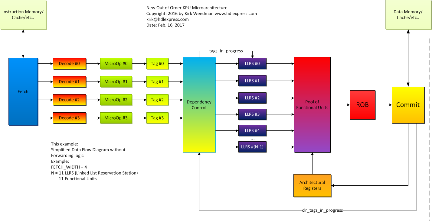
Latest Block Diagrams are shown below. I first began thinking about this design on Mar 2, 2016.
Right click and open or save to see hi resolution/full resolution
More details on specific modules: 4/27/2019
| Module Name | Description |
|---|---|
| KPU_OoOe.pptx | PowerPoint presentation: overview and details about how this new microarchitecture works |
| top_tb1.sv | Top level test bench |
| Include Files | |
| alu_params_RV.h | ALU decode logic parameters |
| cpu_params_RV.svh | localparams determined by RV_params. These should not be changed. |
| cpu_structs_RV.svh | Data structures used by many modules |
| functions.h | Verilog function bit_size() used throughout design |
| instr_pkg.svh | Defines for all RV32 instruction decodes - includes Compressed and others |
| logic_params.h | Includes TRUE, FALSE |
| RV_params.svh | Parameters changable by the user to change the CPU design |
| Source files | |
| afu.sv | ALU Functional Unit. Contains alu_core_RV.sv plus interface to fu.sv |
| alu_core_RV.sv | Logical functions, add, subtract, etc. logic. |
| arch_reg_dep.sv | Architectural Register Dependency logic. The whole reason this project was created was to test this logic which creates a new Dynamic Instruction Scheduling algorithm! |
| bfu.sv | Branch Functional Unit. Contains br_core_RV.sv plus interface to fu.sv |
| br_core_RV.sv | Branch logic |
| CLINT.sv | Core Level Interrupt Controller for RISC_V Machine/Supervisor/User modes |
| clr_dep.sv | Clears certain dependencies when certain instructions retire under certain conditions |
| commit.sv | This commits/retires instructions (multiple per clock if available) In Order. Aso generates some exceptions |
| csr.sv | Control & Status Register logic for M, S, and U modes |
| csr_const.sv | Used to create/instantiate ceratin types of CSR registers |
| csr_lo_cnt.sv | Used to create/instantiate certain types of lower 32 bit counter CSR registers |
| csr_std_wr.sv | Userd to create/instantiate just the write logic portion of some standard type CSR registers |
| decode.sv | top level of decode. Instantiates IPC_NUM decode_core_RV.sv modules as determined by RV_params.svh |
| decode_core_RV.sv | Decode logic for RV32IMC instructions. |
| div.sv | Integer Divide & Remainder logic |
| fetch.sv | Fetches instructions from the L1_ICache. Can fetch multiple branch blocks |
| forwarding.sv | Handles register forwarding logic to improve speed of CPU |
| fu.sv | Dispatches instructions to appropriate functional unit. |
| gpr.sv | CPU architectural register read/write logic. The commit stage writes to this architectural register set. |
| idrfu.sv | Integer Divide/Remainder Functional Unit. Contains idr_core_RV.sv plus interface to fu.sv |
| idr_core_RV.sv | Integer divide and remainder logic. Uses div.sv |
| imfu.sv | Integer Multiply Functional Unit. Contains im_core_RV.sv plus interface to fu.sv |
| im_core_RV.sv | Integer multiply logic - uses vedic_mullt16x16 and vedic_mult_32x32 |
| kpu_core.sv | Top level module of the cpu. Ties all CPU design related modules together. |
| lsfu.sv | Load/Store Functional Unit. Calculates address used by load/store |
| ls_addr_dep.sv | Determines L/S address dependencies |
| pipe.sv | creates a set of registers (based on a data type and size) used in pipelining data |
| rs.sv | Reservation Stations (not similar to any known RS). This is a circular bin of instruction information, stored in instructions order. This module keeps track of all instructions and whether they are ready to start execution. Instructions can execute out of order by going to the appropriate functional unit and the results come back into the appropriate bin (still in order). This module also determines Load/Store address dependencies and whe Load/Store instrucitons may execute. Dependency control logic is now integrated into this module. Basically this module consists of some logic plus the following module instantiations with connections between them: update_ib.sv, fetch.sv, decode.sv, arch_reg_dep.sv, forwarding.sv, fu.sv, ls_addr_dep.sv, clr_dep.sv and commit.sv |
| scfu.sv | System CSR Functional Unit. Contains CSR rd,wr, data, etc. signals used by csr.sv |
| sync_fifo.sv | Synchronous fifo used in design... |
| update_ib.sv | Update Instruction Bins logic. Data in bins is updated by various modules sending data/ctrl logic to this module. |
| spfu.sv | Single Precision Floating Point Functional Unit. Not currently needed for RV32IM version. ***not yet created*** |
| vedic_mult16x16 | unsigned 16 by 16 integer multiplier |
| vedic_mult32x32 | unsigned 32 by 32 integer multiplier |
| Debugging files | |
| disasm.sv | Used for debugging. It displays RV32IMC instructions in assembly language format in ModelSim simulation waveforms. |
| Logic used by KPU Core for simulation | |
| L1_icache.sv | Level 1 Instruction Cache - 8-way set associative, read only 32KB cache with multi-branch predecode |
| L1_dcache.sv | Level 1 Data Cache - 8-way set associative, Write-back 32KB cache, multi-ported |
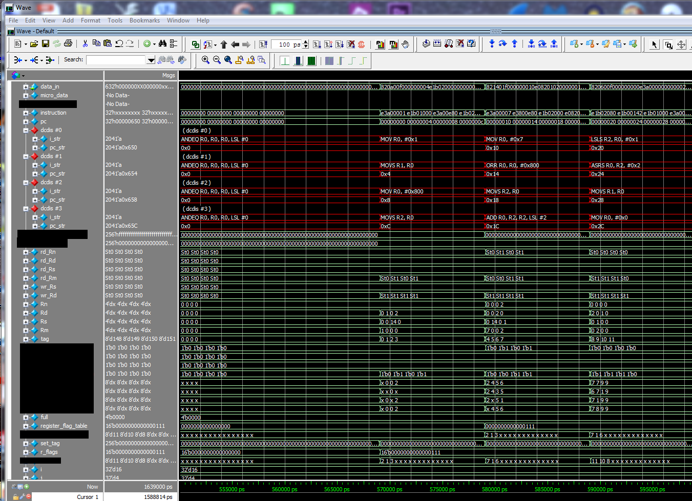
June 4, 2019: Updates to L/S, Commit, and branch logic as well as other updates. Small C programs are starting to run.
April 24, 2019: Addition of ECALL and EBREAK logic
April 24, 2019: Load/Store version 3. Changed logic and found problems I had with previous versions of L/S logic and dependency logic. Also fixed the problem that occured when code "wrap around" occured in the instructions bins.
April 4, 2019: Load/Store updates/fixes, CSR, interrupts, and memory decoding improvements. Code is starting to run. Currently adding multi-ported L1 D$ so that more than 1 L/S can occur. Initially, any Read Hit will respond for any port. This change involves CPU and L1 D$ logic.
Nov 16, 2018: Working on creating various CSRs and interrupt logic. Also added logic to the L1 Instruction Cache related to the incoming cache line data. Multiple instructions per cache line are predecoded to determine which ones are branches and the type of branch. This extra data is saved in the cache for use by new Fetch logic. Looking at a new branch method for Fetch logic which will affect the RS.sv module.
June 13, 2018: Rework of design to simplify/reduce the amount of logic by creating a new "Reservation Station" While the RS can execute instructions Out of Order, it mantains and commits the instructions In Order. Due to the new algorithm, no register renaming is needed and only architectural registers are needed.
May 27, 2018: Some work on the L1 Data Cache. Written for single port input/output. It appears to be working for a single port design. Next goal is to try to create a multi-port design. Still busy with my contract work which will end by the beginning of July 2018.
Nov 2017 - Present: Most all interns busy with college work and I took a short term contract to do some Clock Domain Crossing, Reset Domain Crossing and Re-convergencve debugging/fixing of a system in Redmond, WA. Hope to be back full time on this project by mid to late Spring.
Oct 2017: Following files are being tested or created by interns
LLRS functional testing is underway
L1 Data Cache RTL being designed
L1 Instruction Cache RTL being designed
alu_functional_unit functional testing is underway
Fetch unit RTL is being designed
Single Point Floating Point unit RTL is being designed
Aug-Sept 2017: Guiding and helping volunteer interns, under NDA, working on various projects to support the design and debug of the CPU. No one has info or access to the critical sections of code related to the TIP algorithm (dependency_control.sv and ls_dependency_control.sv) due to it not being patented yet.
July 2017: Decided to get some help. Setting up projects for various engineers to work on relate to this CPU.
June 2, 2017: Debugging new logic related to changes in pool.v and ls_process.v Also debugging ROB and COMMIT stages.
May 15, 2017: Debugging instruction flow through the various stages. Fixes to decoding, disassemble, and the dependency control so far.
May 11, 2017: Debugging RISC-V instructions/disassembler. Created a new Load/Store Process diagram. Added a 32x32 integer multiplier and logic to the ALU for various integer multiply instructions.
Apr 27, 2017: Decided to change from using the ARMv7 ISA to the RISC-V ISA for this new microarchitecture. It will be simpler to implement. Working to implement the RV32I for now.
Apr 19, 2017: Worked on new block diagrams and updates to the PPT presentation.
Apr 17, 2017: Worked on writing lsrs.v and corrected other files under ls_process.v so they all now compile without errors. Stilll need to debug L/S Process block (ls_process.v and all under it). I've also been taking a look at the RISC-V. It looks very interesting and would simplify the design (compared to using this ARM ISA I'm currently using). I will most likely target my new architecture to the RISC-V ISA someday.
Apr 16, 2017: Began writing lsrs.v and cleanup on other modules in ls_process.v
Apr 13, 2017: Most of ls_queue.v and ls_dependency_control.v are written and ready to start debuging. Code for the Pool of Functional Units was removed from kpu_oooe.v and put in its own module as well as cleaned up a bit. Modified Pool block diagram and created new LS Process block diagram.
Apr 11, 2017: Redesign of Pool of Functioanl Units and L/S instructions process.
Mar 28, 2017: Removed the Pool of Functioanl Units diagram related to ARMv7 ISA becuase of a design problem.... back to the drawing board on the load/store section :(
Mar 27, 2017: The following diagram for the Pool of Functional Units reflects the architecture needed for an ARMv7 type ISA where the address is not known (i.e. calculated) until inside the Load/Store Functional Unit. Once the L/S address is known, the information from all Load/Store Functional Units are fed into the L/S Dependency Control. This module caluclates address dependencies in a similar way that the Dependency Control module calculates register dependencies. Output data from the L/S Dependency Control module is placed into an available Load/Store Reservation Stations (LSRS). These reservation stations hold the instruction from starting a load or store from/to memory until all dependencies are satisfied, much like the Linked List Reservation Stations do for the architectural registers. Once a Load/Store instruction is released from an LSRS it can then start a Load or Store transfer from/to memory. The instruction then passes on to the ROB and Commit units as do ALU type instructions. Also updates to the KPU design PowerPoint Presentation were made today. It's basically finished.
[pool of functional units diagram for armvy removed from here becuase of design problem]
Mar 23, 2017: I think I've finally determined how I want to do Load/Store logic in this new architecture as well as how to do it for the ARMv7 ISA. The above Pool of Functional Units diagram will get changed soon to show the implementation as it would relate to the ARMv7 ISA. Load/Store address dependencies will get handled in a similar way as the register dependencies. ...stay tuned... Muhammad Moazam is on board now and will start createing testbenches for simulation for a new module I created called ls_cam_cache.v which will be used to hold load/store addresses and tags in a CAM (Content Addressable Memory) type manner.
Mar 20, 2017: Created a simplified block diagram of an example of the Pool of Functional Units. The actual POOL is determined by parameters that can be changed. The number of each type of Functional Unit can be changed.
Mar 10, 2017: Finished the basics of module ls_cam_cache.v. Now it needs debugged before adding the final bit of code it needs. Engineer Muhammad Moazam has volunteered to help do some debugging in exchange for the experience.
Mar 8, 2017: Creating a CAM (content addressable memory) type cache that will hold Load/Store addresses and any associated Tags. Dependencies related to addresses will be handled in a manner similar to how dependencies related to registers (and their assocoated tag) are handled in this new architecture. CAM entries are also sorted using a linked list method that will have its most recently used address at the beginning of the linked list and its least recently used address at the end of the linked list. Once the cache becomes full and a new address needs to be put into the cache, the cache will overwrite (assuming the entry is not in active use) the last entry with the new addresss/tag and put it at the beginning of the linked list as being the most recently used. Each address saved in the cache is unique - i.e. no duplicate addresses
Feb 28, 2017: Temporarily sidetracked since the 16th with another project I have to finish up.
Feb 16, 2017: Conversion to System Verilog mostly complete and simulations working again. Separated ROB/COMMIT code and fixed a couple bugs due to both being together in the same module.
Right click on the pic and save or open in a new tab to see the full resolution.
Feb 12, 2017: Decided to change all code to use System Verilog features. Found a couple of coding bugs doing this. Working to get simulations working again. (It was working before converting to System Verilog)
Feb 7, 2017: Nearing completion of writing code for the Load/Store logic. Need to create an L1 cache that will interface to the Load/Store logic.
Jan 29, 2017: Updated the PPTX presentation. Worked on a new Load/Store logic. This will soon be integrated into the last stage of the design.
Jan 16, 2016: Updates/fixes to forwarding logic has greatly improved IPC. For the test being used (186 instructions completed in 47 clocks, hardware ignoring branches & load/store instructions), the IPC is close to 4 for a 4 instruction wide issue. The LLRS queues are only averaging 1 or 2 instructions in them up until where the test has a lot of back to back load/store type instructions. This backup is at least partially due to no forwarding logic for load/store instructions yet. There may be some other instructions doing this too. Anyway, the forwarding logic currently implemented seems to be working much better. More work on the powerpoint presentation about this design.
Jan 10, 2016: To facilitate multiple micro-ops due to a single instruction, the microarchitecture has been changed to the following.
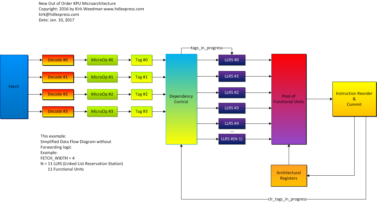 Right click on the pic and save or open in a new tab to see the full resolution.
Jan 6, 2016: Spending time determining how to issue multiple micro-ops due to a single CPU instruction.
Jan 5, 2016: Spent time debugging/fixing commit.v logic and related ALU problems.
Jan 4, 2016: Found that I had a parameter that was wrong and some of the LLRS units where not getting data. Fixed it and now IPC = 256 instructions in 73 clocks = IPC of 3.5 for a 4 issue wide CPU. Still appears to be another problem slowing it down, but things are getting better. The simulation test used is a random wide variety of instructions with no Load/Store delay penalty and no branch delay penalty so the IPC should be VERY close to 4 for this 4 issue wide CPU simulation setup. Currently the L/S and branch instructions are decoded and processed up to the Functional Unit related to them, but they are basically discarded until I have time to work on them.
Jan 3, 2016: Register forwarding updates/fixes. Microcode table updates/fixes. However I'm only getting 258 instructions is 111 clocks = IPC of 2.3 for a 4 issue wide CPU. I can see where the problem lies. Just need to figure it out.
Jan 2, 2016: Basically finished with new integer multiplier section of the ALU. Here's a simple block diagram of what was implemented.
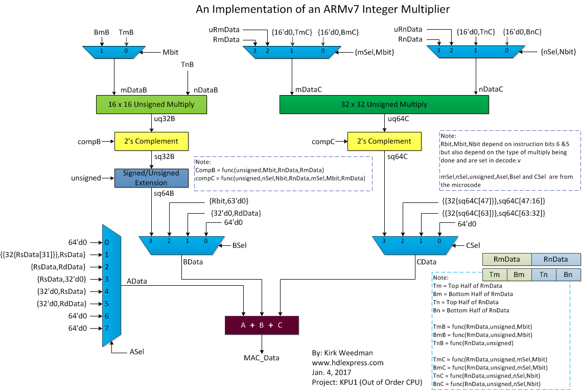 Updated Jan4. Right click on the pic and save or open in a new tab to see the full resolution.
Dec 30, 2016: Overhauling the integer multiplier section of the ALU to maximize resources and fix problems. Removed one of the multipiers. Only uses one 16x16 unsigned multiplier and one 32x32 unsigned mutiplier.I may post a block diagram here when finished.
Dec 28, 2016: Added more ARM Media instruction microcode, debugged various microcode. Fixes to transfer logic from LLRS to Functional Units. Added simulation debug code to arm_micro.v to abort sim if a certain invalid type of microcode is used (pulled from table). Found a few instances of this problem and corrected logic.
Dec 26, 2016: Created a Xilinx ISE project and compiled the Verilog modules to see if I had any RTL problems. A few things had to be changed to be synthesizable. Created a new simplified block diagram that is now in my PPT presentation.
Dec 23, 2016: Worked on the load/store functional unit (ls_functional_unit.v) and related logic in the whole system. Still have a chunk of logic related to Load/Store to go into the final Commit stage. Updated microcode table in arm_micro.v related to load/store instructions.
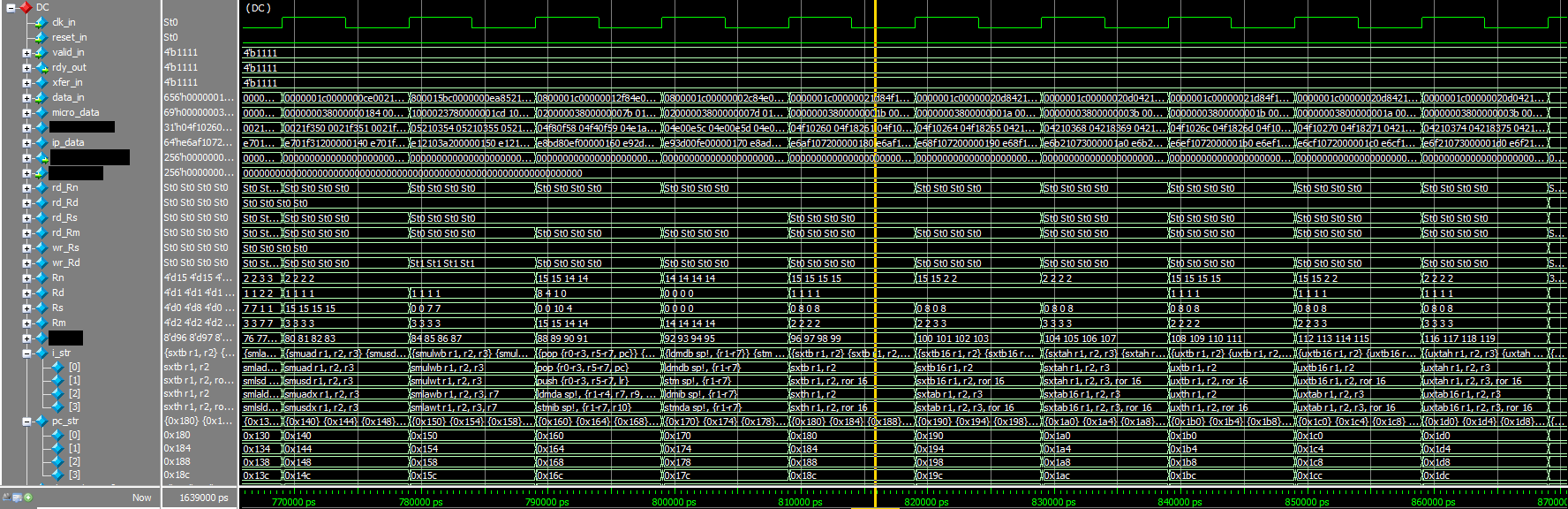
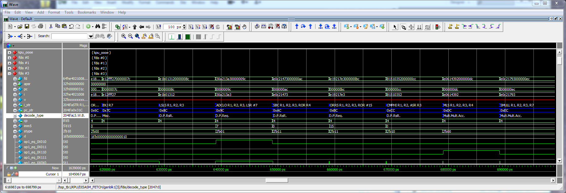
Dec 22, 2016: Continuation of decode,microcode and disassemble fixes. See bottom signals in waveform below
 Right click on the pic and save or open in a new tab to see the full resolution.
Dec 20, 2016: Worked on microcode table and logic for ARM "Extra load/store" instructions. Continued PPT presentation - 45 slides so far.
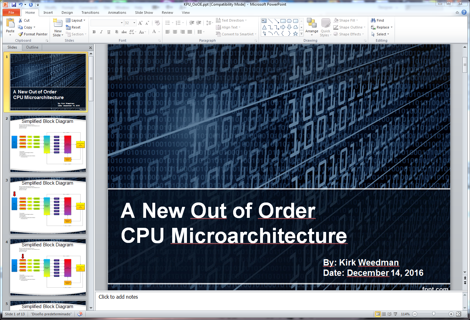
Dec 14, 2016: After months of having random booting issue after a poweron, my desktop computer finally died today :(. After trying to figure out the problem, I discovered the Power Supply voltages were all very low! Drove in the afternoon snowstorm to Fry's in Wilsonville, OR to get a new supply and put it in. Its working again and not having the boot issue. Started creating a powerpoint presentation about this new Out of Order Execution microarchitecture.
 Right click on the pic and save or open in a new tab to see the full resolution.
Dec 13, 2016: Started working on the Load/Store Functional Unit and microcode control logic. Fixed a couple issues with decode.v.
Dec 11, 2016: Completed adding ARM 32 bit Media Instructions to armv7_disasm.v. Currently the architecture does not yet incorporate any THUMB instructions and probably won't for awhile as the real goal is to show the new Out of Order microarchitecture being able to work. Debugged 200+ different instructions from various types (Data Processing Register, Data Processing Register-shifted Register, Misc., Data Processing Immediate, Halfword multiply and multiply accumulate, multiply and multiply accumulate, Sync. Primitives, Extra Load/Store, Branch, etc..)
Dec 8, 2016: Added most of the ARM 32 bit Media Instructions to armv7_disasm.v.
Dec 6, 2016: Changed armv7_disasm.v. Changed the disassembler code to use SystemVerilog "string"s instead of a method with regular Verilog. It shortened the code a bit. Spent the day adding new instructions and debugging them. Still need to add Media instructions. Being able to SEE the instruction flow during simulation is a big help.
November 29 - Dec 5, 2016: Microcode table data fixes and improvements to the microcode state machine/instructions. Feedingvarious instructions to armv7_disasm.v and debugging them. I use the results to also check decode.v functionality. This will take a lot of time.
 Right click on the pic and save or open in a new tab to see the full resolution.
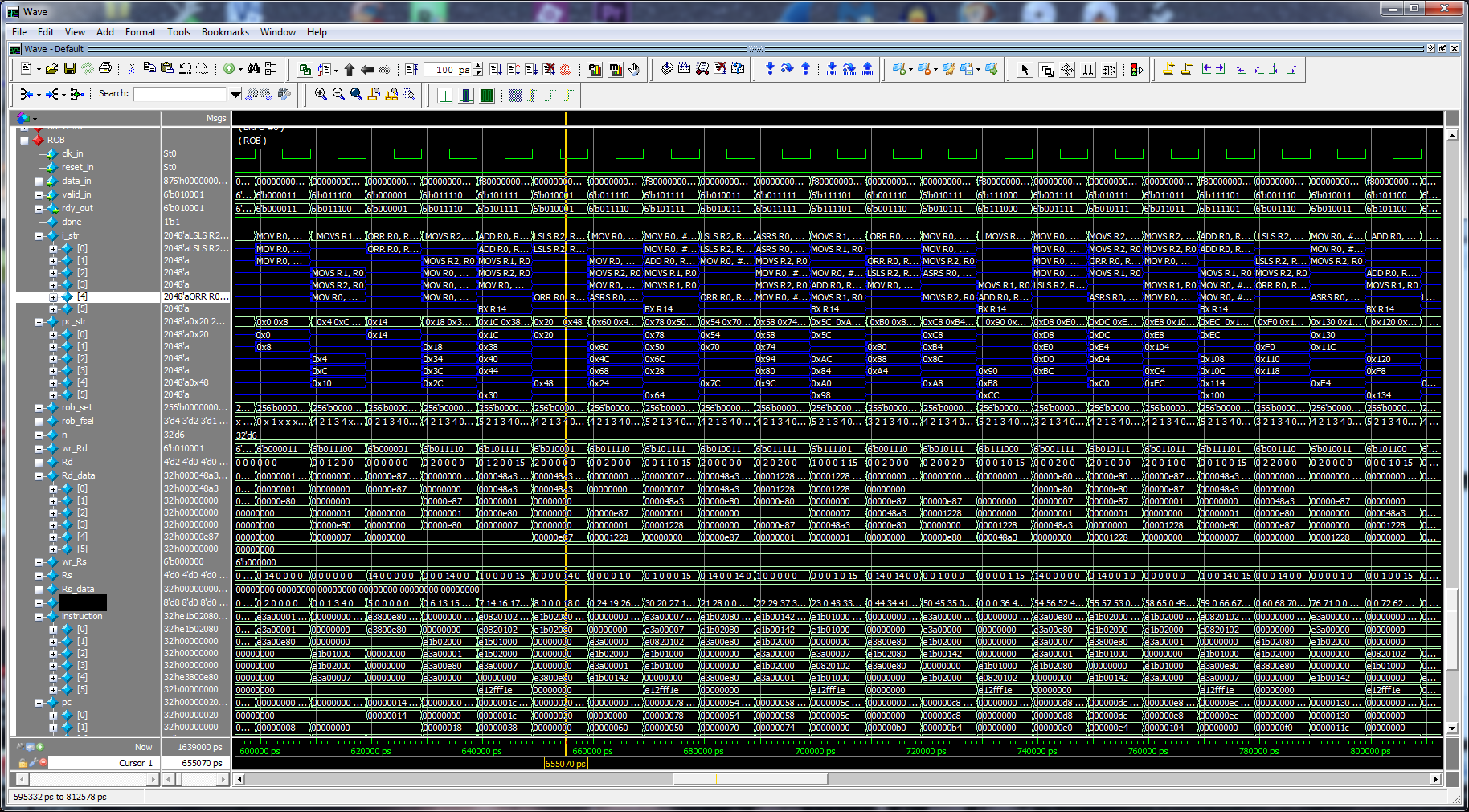
November 27, 2016: Bugs found and fixed. Got first 100 instructions executed in 31 clocks. Still needs more forwarding logic. The following pic shows the instruction flow in the ROB/Commit section using my ARM disassembler in the simulation. Right click on the pic and save or open in a new tab to see the full resolution.
November 24, 2016: Found out why the CPU appeared to be going very slow - no forwarding logic. Added one (of 3 I need to add) level of forwarding from the ALU Functional Units back to the LLRS stage. The commit.v now has a Reorder Buffer and then commit logic before data is written back to the architectural registers. Thus forwarding logic will get added for the ROB and the COMMIT stages once I get other debugging done.
November 20, 2016: Ran into a dependency algorithm problem. May take some time to figure this one out.
November 18, 2016: Anther fix to llrs.v to correct what happens when both a trasfer in and out of the module occur at the same time. Also some minor fixes to commit.v and kpu_oooe.v. Today was the first day that the first instruction made it all the way through the architecture. Unfortunately nothing else did... Debugging is going well.
November 17, 2016: Starting creating br_functional_unit.v so that branches dont get stuck in the llrs.v units while debugging. For now I'll just bring them into the br_functional_unit.v and pass them on to commit.v so they can be retired and not hold up data processing instrucutions I'm currently debugging.
November 16, 2016: more debugging of llrs.v (problems with adding/removing data in linked lists), dependency_control.v and just about to start debugging llrs.v - commit.v interactions.
November 14, 2016: llrs.v is beginning to work. Still different test cases need simulating. In the picture below, I created some special Verilog code just for debugging the linked lists. Look at the "used_str" and "unused_str" signals. These directly correlate to two singly linked lists called "used" and "unused" Both lists use a single array, but have pointers that separate which entries are in which list (used or ununused). The special verilog code goes through both lists and creates ascii strings that can be displayed to show the linking order of both lists during simulation. This was a great way to debug the actual RTL code to know if my linked lists were working properly and that all links are updated correctly. Each time a CPU instruction is saved it takes an "unused" entry and links it into the "used" linked list. Not shown, but yet to test will be when an instruction is removed and a "used" entry goes back to the "unused" list. There is no data physically moved, just linked list pointers (values) get updated. In debugging of the architecture, the original 32 bit instructions are passed to each stage along with microcode and other signals. What is not shown here is all the microcode and various signals saved in the linked lists corresponding to the instructions that are being used. For the final version (RTL only) all the debug and instruction passing will not be compiled into the design. In this particular simulation display, it is showing 1 of the 6 llrs.v modules, with each having an instruction queue depth of 8 (parameter can easily be changed to 64, 256 or whatever is needed)
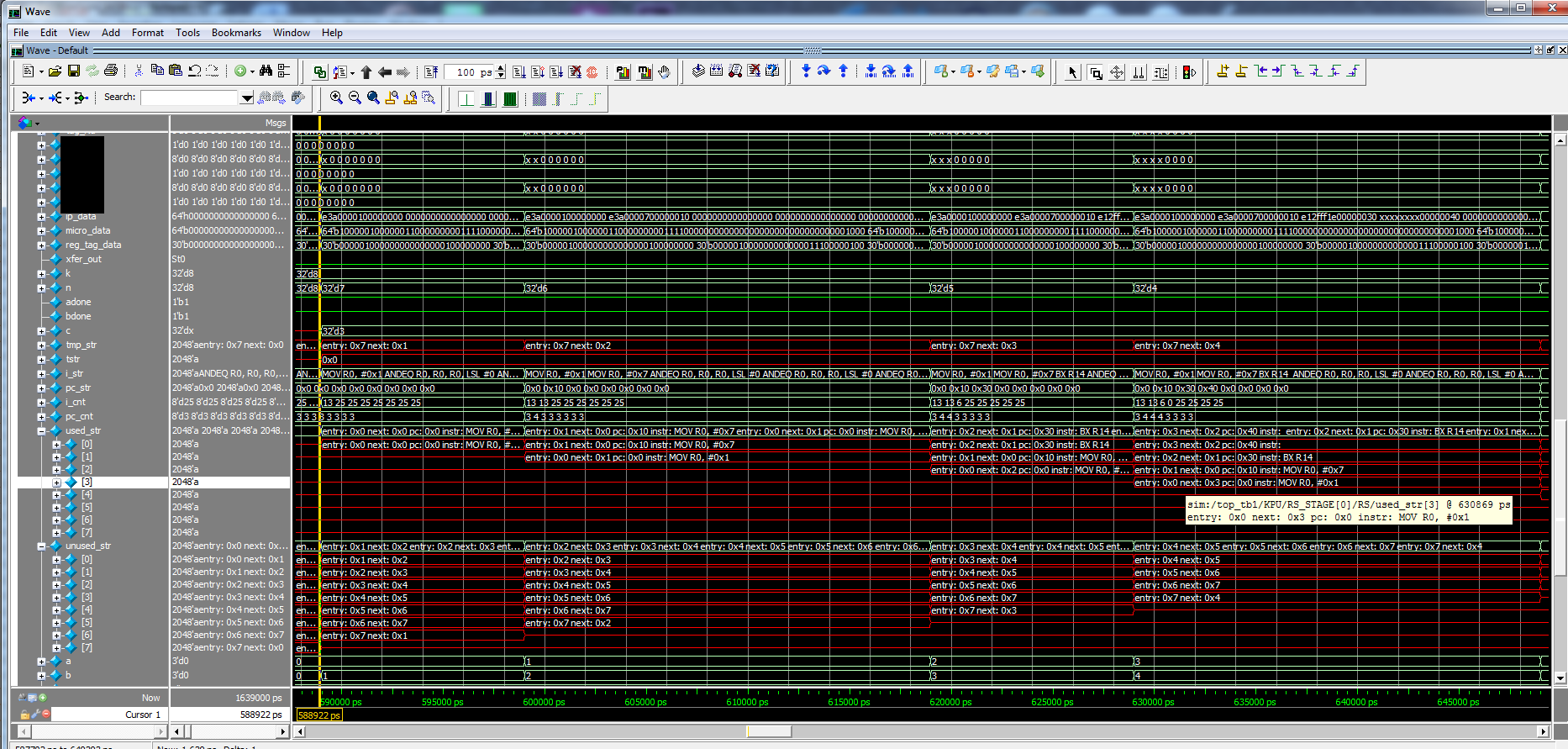 right click on pic and either save or view in a new tab to see the full resolution
November 10, 2016: Fixes to llrs.v logic. Looking much better now.
November 9, 2016: Working on DC - LLRS flow/control logic. Snapshot below (open in another tab to see full size) of the Dependency Control unit working on 4 instructions per clock. This can easily be changed to 8 ... 64... by changing 1 parameter. Similar changes to other modules have to be made.
November 7, 2016: Good debugging progress up to DC (Dependency Control). Also updates/fixes to debug_asm.v, which is renamed to armv7_disasm.v. Currently teh parameter determining the number of instructions per clock is set to 4. Most everything is parameterized so it can be easily changed. Things such as IPC, the number of LLRS units, instruction window length, the number of different types of functional units, etc.. This will make it easy to try different CPU design configurations later on.
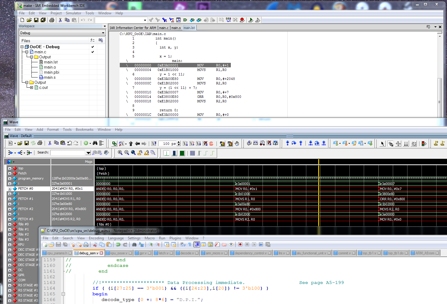
November 4, 2016: Currently debugging debug_asm.v, fetch.v, etc.. Right click on the pic below and save it so you can see the full hi res pic. This shows the beginning of debugging instructions using the debug_asm.v module in a ModelSim simulation. If anyone is interested in helping debug this module and using it, contact me. You will need ModelSim and a tool such as IAR Workbench to compile code to generate assembly language to compare against ModelSim, and binary code (in hex format) that can be placed in a file that the simulation can read in.
November 2, 2016: Wrote simple testbench top_tb1.v and started the debugging process. Typical bugs like port size mismatches between modules, wire vs. reg usage on port signals, etc... Still more to debug before I can actually get the simulation (waveforms) running so I can debug the logic.
November 1, 2016: Wrote commit.v, updated gpr.v and kpu_ooe.v
October 31, 2016: Added new ALU control bits to microcode ROM/RAM table and logic, added Multipliers and logic in alu_functional_unit.v, got logic completed for ARM Data Processing instruction flow from Fetch through Issue/Execute ready to begin debugging once I create a testbench.
October 26, 2016: Worked the ALU logic used in alu_functional_unit.v, microcode ROM/RAM table and logic, decode.v logic updates
October 18, 2016: For debugging purposes I am optionally passing the full 32 bit instruction through each stage. I'm creating a Verilog code module that can be used to disassemble the instructions at various locations and display in ModelSim the disassembled instructions as as ASCII string in the waveforms. This will greatly help watching the data flow.
October 13, 2016: Various code mods. Renamed Hazard Control to Dependency Control.
October 9, 2016: Got all but the ROB/commit module (not designed yet) to compile without errors. Next I'll start making testbenches for individual modules and the whole design.
October 5, 2016: It's started raining here in Oregon so I've been inside the last couple of days and made good progress and improvements on the Fetch, Decode&Tag, Hazard/Control, and LLRS sections shown above. I may rename some sections as this is a very different architect for Out of Order type CPUs. One important change to the above diagram is that there are now more LLRS blocks than the number of instructions Fetched per clock (Decodes too). The ROB/Commit section will be able to retire more instructions per clock (if available and can be done) than there will be instructions Fetched per clock. This will help improve IPC as some instructions may have to wait awhile (i.e. Loads, Stores,etc..) in the LLRS blocks before they are ready to be executed.
August 24, 2016: Spent several hours (out of the last month since last reporting) working on the Register Rename block above, but discovered a new method that looks promising. For now I'm calling it Hazard Control. Like register renaming methods, it eliminates WAW & WAR hazards. It keeps track of instruction dependencies but doesn't rename registers and/or allocate a new set of physical registers. So far, the logic appears to be simpler than typical renaming techniques. The goal is something simpler (in terms of logic levels which determine min. clock cycle widths) because I want to eventually make the issue width much larger than 4. I hope to be able to devote most of my time on this starting by the end of October. For the last 4 months I've had other obligations. :(
| 0 | 1 | 2 | 3 | ---> | Decode & Tag #0 | ---> | Hazard Control | ---> | LLRS #0 | ---> | Issue/Execute | ||
| Decode & Tag #1 | ---> | ---> | LLRS #1 | ---> | ROB/commit | ||||||||
| Decode & Tag #2 | ---> | ---> | LLRS #2 | ---> | -----> | ||||||||
| Decode & Tag #3 | ---> | ---> | LLRS #3 | ---> | |||||||||
| ... | ... | ||||||||||||
| ---> | LLRS #M | ---> | |||||||||||
| ... | ... | ... |
July 22, 2016: Finished initial design of the LLRS (Linked List Reservation Stations) module (llrs.v) and have most of the Reg. Rename (reg_rename.v) module written that will do register renaming logic for the new ARM OoOE cpu.
// Example: N = 4 wide instruction fetch
| 0 | 1 | 2 | 3 | ---> | Decode & Tag #0 | ---> | Reg. Rename #0 | ---> | LLRS #0 | ---> | Issue/Execute | ||
| Decode & Tag #1 | ---> | Reg. Rename #1 | ---> | LLRS #1 | ---> | ROB/commit | |||||||
| Decode & Tag #2 | ---> | Reg. Rename #2 | ---> | LLRS #2 | ---> | -----> | |||||||
| Decode & Tag #3 | ---> | Reg. Rename #3 | ---> | LLRS #3 | ---> | ||||||||
| ... | ... | ... |
Decode & Tag - Instruction decoding and "tag" creation. The tag "magic" happens in LLRS and ROB/commit.
Reg. Rename - The number of physical registers is parameterized and can be changed to get the best performance per application. Currently it's set to 64. reg_rename.v keeps track, using a linked list, to which of the physical registers are the current architectural registers defined by the ISA.
LLRS - a new type of Linked List Reservation Station. The first CPU version will not be superscalar as shown above, but will be designed & parameterized so that it can become a superscalar. There are two linked lists that use a common pool of Reservation Stations. One linked list is "used" pool items and the other linked list is the "unused" pool items. Only 1 clock cycle is needed by the module due to the way the linked lists are maintained. The "used" linked list keeps ready instructions in order from oldest to youngest so that the oldest can be passed on to Issue/Execute first.
Issue/Execute - contains a pool of execution resources (non floating point for the first version) usable by all available instructions issued per clock cycle from the LLRS module(s). Multiple instructions (more than N) can be passed per clock to the ROB/Commit
ROB/Commit can commit multiple (more than N) ready instructions per clock.
July 8, 2016: Worked more on a module that will be the equivalent of a reservation station for the new ARM OoOE cpu.
June 24, 2016: Slowly starting to work on the new ARM OoOE architect idea I have as time permits. Just completed writing a new module (A linked list type of Reservation Station) I will need to make sure is synthesizable and then simulate it. I finally found a patent (owned by QualComm) that may have some similarity to my design, but it doesn't have features my design method does.
April 2, 2016: Created a disassembler (for a portion of the ISA) to display the assembly language instructions during ModelSim simulations. Also looking at a another OoOE architect idea. However, I now have to do some other work for the next 2 - 3 months before I can continue on this project.
Mar 22, 2016: Just found out during simulation that my new OoOE architecture has a design problem. So back to the drawing board on that idea. Still working on a new architecture based on the ARM7-TDMI ISA.
Mar. 17, 2016: Decided to go with the ARMv7 ISA for this new Out of Order design. Even though my OoOE internals are very different than ARM's, I guess I can't release the CPU with this ISA. I also have some of the basic modules created and they finally, tonight, compile without errors. Currently setting up a test bench and top level to integrate all the current modules and begin debugging. First test will be just to get the basic flow working for all the Data Processing type instructions and see that my new style of logic works. I also setup IAR tools for ARM to generate binary code to use in my Verilog simulations.
Mar. 9, 2016: Modified ISA for both KPU55 and KPU_OoOE. Working on creating KPU_OoOE CPU with Branch Method 3. Modifications to DECODE stage so that it may be easy to change it to use microcode instead of brute force decoding for every instruction. It would also facilitate changing over to a different ISA - such as an ARM Cortex. The microcode method will reduce the amount of logic gates in the DECODE and thus reduce delays in the stage. Might be nice to show this CPU running on an ARM instruction set. Anyone have any suggestions?
Mar. 2, 2016: In researching how these branch methods may apply in OoOE processors, I've gotten sidetracked today with a new algorithm I came up with for OoOE that I believe is easier to implement than Tomasulo's. I've begun creating a new OoOE CPU to see if it's any good.
unique visitors since Nov. 14, 2016